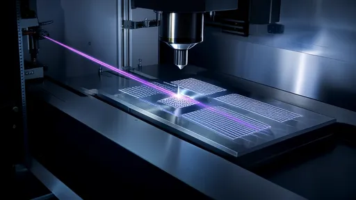
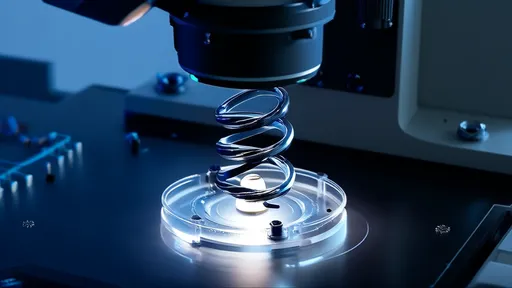
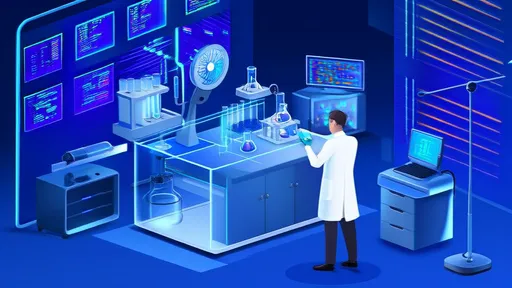
The world of photonic crystals has taken a revolutionary leap forward with the advent of femtosecond laser fabrication. This cutting-edge technique allows for the precise construction of intricate photonic structures at the nanoscale, opening up unprecedented possibilities in optics, telecommunications, and quantum computing. Unlike traditional manufacturing methods, femtosecond lasers offer unparalleled control over material modification, enabling the creation of complex periodic dielectric structures that manipulate light in ways previously thought impossible.
At the heart of this technology lies the unique interaction between ultra-short laser pulses and matter. When a femtosecond laser pulse (lasting mere quadrillionths of a second) interacts with a material, it induces nonlinear absorption processes that modify the material's refractive index with extraordinary precision. This non-thermal process allows for the direct "writing" of photonic crystal structures inside transparent materials without causing collateral damage to surrounding areas. Researchers have successfully fabricated both two-dimensional and three-dimensional photonic crystals with lattice constants matching the wavelength of visible and near-infrared light.
The implications for optical computing are particularly profound. Photonic crystals created through femtosecond laser writing exhibit complete photonic band gaps - ranges of frequency where light cannot propagate through the structure. This property enables the creation of optical circuits where light can be guided, split, and manipulated with minimal loss, potentially revolutionizing data processing speeds. Recent experiments have demonstrated light confinement in cavities smaller than the wavelength of light itself, a crucial requirement for dense optical integration.
In telecommunications, femtosecond-fabricated photonic crystals promise to overcome current bandwidth limitations. The ability to create defect modes within perfectly periodic structures allows for the design of ultra-narrowband filters and wavelength division multiplexing components with unprecedented channel density. Moreover, the third-order nonlinearity inherent in these structures enables all-optical switching at speeds measured in femtoseconds, far surpassing what electronic components can achieve.
Quantum technologies stand to benefit enormously from these advancements. The precise positioning of defects in photonic crystals creates ideal environments for trapping and manipulating quantum dots or nitrogen-vacancy centers in diamond. Such systems could form the backbone of future quantum networks, enabling the generation, storage, and transmission of quantum information. Researchers have already demonstrated quantum entanglement between photons mediated by femtosecond-written photonic crystal structures.
The fabrication process itself continues to evolve rapidly. Adaptive optics systems now compensate for aberrations during deep subsurface writing, while computational inverse design algorithms help create photonic crystals with customized optical properties. The latest generation of femtosecond lasers offers repetition rates in the MHz range with pulse energies precisely controlled at the nanojoule level, enabling high-throughput fabrication of photonic crystal devices.
Material science has kept pace with these technological advances. Beyond traditional glass substrates, researchers are now writing photonic crystals in biocompatible polymers for medical applications, in nonlinear optical crystals for frequency conversion, and even in phase-change materials for reconfigurable photonic circuits. The marriage of femtosecond laser fabrication with emerging materials promises to unlock functionalities that could transform photonics in ways we are only beginning to imagine.
As the technology matures, challenges remain in scaling up production and improving reproducibility. However, the unique advantages of femtosecond laser writing - its flexibility, precision, and compatibility with diverse materials - position it as a cornerstone technology for the photonic age. From ultra-efficient solar cells to invisible cloaking devices, the applications of laser-fabricated photonic crystals span across industries, promising to reshape our technological landscape in the coming decades.
The convergence of femtosecond laser technology with photonic crystal design represents more than just an incremental improvement in fabrication techniques. It embodies a paradigm shift in how we control and manipulate light at the most fundamental level. As research institutions and industrial laboratories worldwide continue to push the boundaries of what's possible, we stand at the threshold of a new era in photonics - one where light is sculpted with atomic precision to serve our most demanding technological needs.
By /Aug 5, 2025
By /Aug 5, 2025
By /Aug 5, 2025
By /Aug 5, 2025

By /Aug 5, 2025
By /Aug 5, 2025

By /Aug 5, 2025
By /Aug 5, 2025

By /Aug 5, 2025

By /Aug 5, 2025
By /Aug 5, 2025
By /Aug 5, 2025
By /Aug 5, 2025
By /Aug 5, 2025
By /Aug 5, 2025
By /Aug 5, 2025
By /Aug 5, 2025

By /Aug 5, 2025

By /Aug 5, 2025
By /Aug 5, 2025